Electronic Timer Part1
Introduction
For once, we are not going to talk about networking or system or automation.
Let’s talk about…
Electronics !
I found this very old electronic circuit from high school time. It is an educational electronic circuit designed to teach students about digital electronics.
I thought it would be interesting to try to explain how it is working and on top of that, as it is defective, I will also have the opportunity to write a little bit about troubleshooting.
I will do my best to try to explain it so you would understand regardless of your electronic knowledge/background.
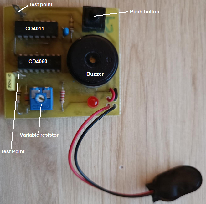
Here is a picture of the electronic circuit below. It is basically just an electronic timer.
It works with a 9V battery.
As soon as you plug the battery, the red LED will turn on and the (invisible) timer will start.
When the time is up, the buzzer will emit 4 beeps and then the red LED will turn off.
That’s it.
To use it again, you can press the black button at the top right (it will reset the circuit)
You can set the delay for the timer using a screwdriver to fine tune the blue variable resistor.
Delay can be set from 40 sec to 3 min 30
You can find the same picture without annotations here.
Global diagram
Because it was a very long time ago, I lost the diagram that was provided, but because this circuit is very simple, it was easy to rebuild the diagram by retro-engineering.
Below you can find the diagram with some annotations :
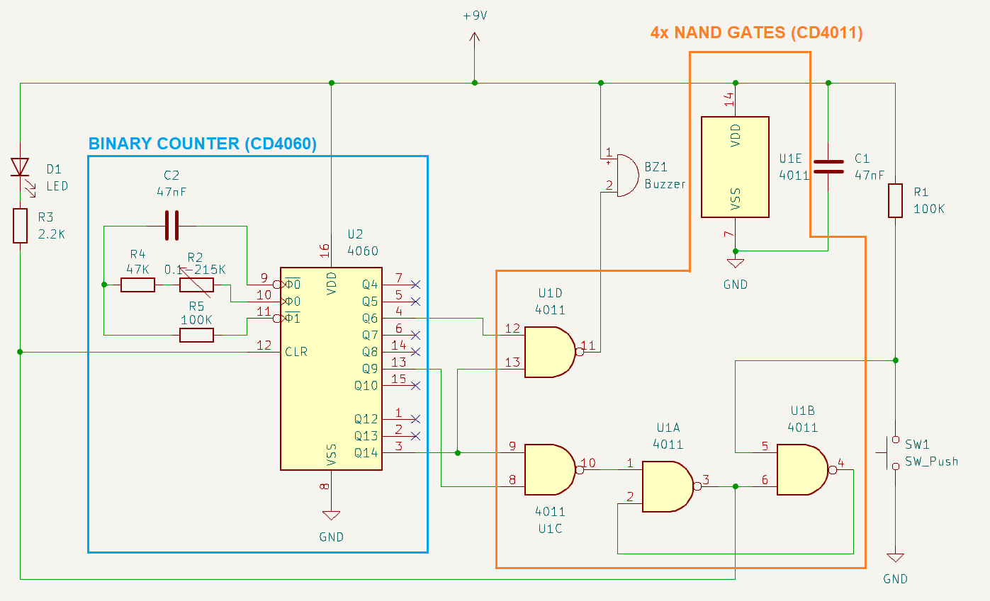
Additionally you can find :
- The same diagram without annotations
- A picture helping you to understand which component is what based on the picture)
We will now deep dive into what these two majors IC are doing but in a nutshell :
-
CD4060 : Counting (this is the heart of the timer)
-
CD4011 : Those are NAND gates, in this case they allow to trigger other components like the LED (light) or the buzzer (sound) based on the outputs of the timer (CD4060).
CD4060 - Binary Counter
I cannot go too much in detail about all the feature of the CD4060 (otherwise this article would be even longer), you can either check the datasheet or this site for that.
But basically you need to feed a clock signal to it (using pins 9 to 11) and it will output a different signal on its pin named Q4 to Q14.
What is nice about it, is that :
The output on Q4 will change every 8 clock pulses.
The output of Q5 will change every 16 clock pulses.
The output of Q6 will change every 32 clock pulses.
And it goes like that for all output pins. Q14 will change every 8192 clock pulses.
Back to our educational electronic circuit, lets say you tune the variable resistor to get a clock signal of 100 Hz (=period of 0.01s).
Q4 output, will change every 0.08 sec (8 x 0.01 sec).
Q5 output, will change every 0.16 sec (16 x 0.01 sec).
And so on.
Please refer to the table below.
| Pin | Period (s) | Frequency (Hz) | Half-Period (s) |
|---|---|---|---|
| Clock | 0.01 | 100 | 0.005 |
| Q4 | 0.16 | 6.25 | 0.08 |
| Q5 | 0.32 | 3.12 | 0.16 |
| Q6 | 0.64 | 1.56 | 0.32 |
| Q7 | 1.28 | 0.78 | 0.64 |
| Q8 | 2.56 | 0.39 | 1.28 |
| Q9 | 5.12 | 0.19 | 2.56 |
| Q10 | 10.24 | 0.10 | 5.12 |
| Q11 | 20.48 | 0.05 | 10.24 |
| Q12 | 40.96 | 0.02 | 20.48 |
| Q13 | 81.92 | 0.01 | 40.96 |
| Q14 | 163.84 | 0.005 | 81.92 (1 min 22 sec) |
And if by now you are wondering why I highlighted Q6, Q9 and Q14, this is because these are the outputs that the device is using. Check the diagram again, you will see that only these outputs are connected to the NAND gates of the CD4011.
Important :
Starting from now, I will talk a lot about the state levels LOW and HIGH.
LOW : Usually describe the voltage Ground (0V)
HIGH : Usually describe the voltage VCC (9V in our case)
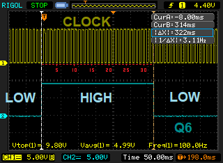
After the CD4060 gets powered, all its output will be initially LOW (0V). Then after 0.32 sec, Q6 will become HIGH (9V), then 0.32 sec after if will become LOW again. And the cycle continue.
Here is an oscilloscope measure showing the clock signal (dark yellow) and Q6 signal (dark blue). Notice how Q6 is changing level every 32 clock pulses (every 0.32 sec [322 ms]).
And about Q14, let’s just say that if you have a clock signal of 100Hz, the buzzer will emit sound after 81.92 sec. You see where I am going with that ;).
We will see in the next part why Q14 alone is not enough to make our circuit work the way we want and why we need both Q6 and Q9 as well.
CD4011 - NAND gates x4
Quick reminder of what will be the output of a NAND gate depending of the value of its two inputs:
| Input 1 | Input 2 | Output |
|---|---|---|
| LOW | LOW | HIGH |
| LOW | HIGH | HIGH |
| HIGH | LOW | HIGH |
| HIGH | HIGH | LOW |
As an easy reminder, the output of the NAND gate will be LOW only if its two inputs are HIGH.
Buzzer trigger
Let’s start by the easiest, the NAND gate triggering the buzzer. Initially the NAND gate output will be HIGH (because both Q6 and Q14 will output a LOW signal)
[Step 1] The reason the buzzer is not spitting sound yet is because both its pins are connected to VCC (pin 11 is HIGH, so at voltage VCC[9V]), so no current can flow.
[Step 2] At some point Q6 will be enabled, but that will not change the NAND gate output.
[Step 3] Later, Q6 will be disabled and Q14 will be enabled, but it still not going to set the NAND gate output to LOW.
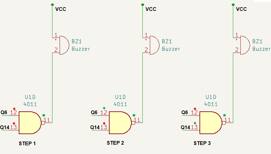
[Step 4] At some point, both Q6 and Q14 will be enabled, this will tied the NAND gate output to ground (LOW). Now current can flow through the buzzer and it will emit sound.
[Step 5 & 6] However shortly after, Q6 is going to be off again, setting the NAND output back to HIGH level, stopping the buzzer. And this cycle is going to repeat a couple of time as Q6 switch between on and off.
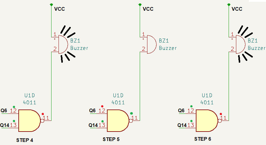
However, if you watch this video, you would probably notice that the buzzer emits beeps only 4 times and then goes to silence.
However, you are probably expecting the sound repeating its cycle for at least during the whole time Q14 is HIGH, right ?
That’s where the reset NAND gates network is playing its role.
Circuit reset
Important:
The reset part will force the CD4060 to go into a “sleep state” where it will stop counting and set all its Qx output to LOW.
To reset the CD4060, its pin 12 (CLR) must be set to HIGH (voltage at VCC).
As soon as the pin 12 is back on GND (LOW), the CD4060 will start counting again.
The sleep state will be disabled as soon as the user press the SW1 button.
If you check on the diagram below, you will notice that Q14 is also used on the circuit reset part.
As I said before, Q14 going HIGH is marking the end of the timer, and the following is designed to happen:
-
Q14 switch from LOW to HIGH => That means the timer is up
-
Q6 switch alternate from HIGH/LOW to make a repeating sound
-
As soon as Q9 is HIGH (and because Q14 is still HIGH), the sleep mode will be activated on the CD4060
So this is why the buzzer sound is not repeating for too long (only 4 times), because at some point Q9 is going to be set to HIGH and put to sleep the CD4060, interrupting everything.
Warning: Less easy part is coming
Let’s have a look at the diagram below to describe the initial state:
-
Left NAND gate:
- Q14 and Q9 are LOW => output is at HIGH
-
NAND gate on the right:
-
Pin 5 is pulled up to HIGH (using the resistance connected to the VCC line)
-
Pin 6 is connected to the output of another gate but in the initial state we can assume it is going to be set as LOW.
-
Output is HIGH
-
-
Middle NAND Gate:
-
Pin 1 is HIGH because of the output of the left NAND gate (Pin 10)
-
Pin 2 is HIGH because of the output of the right NAND gate (Pin 4)
-
Output is LOW (which is also the value on the right NAND gate at Pin 6 so we are back on our feet)
-
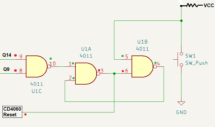
At beginning all Qx output of CD4060 are set to LOW.
Q9 will turn on HIGH first, then LOW => nothing will happen on the left NAND gate
Later Q14 will turn HIGH => nothing will happen on the left NAND gate, but the beeping sound will start as explained in the previous part.
Q9 will turn HIGH again => this time the left NAND gate output will be set to LOW (as all its input pins are now HIGH).
Which in turn will change the state of the middle NAND gate and it will output HIGH.
That last step will create two additional state changes:
-
The reset pin of the CD4060 will now be HIGH, causing the CD4060 to stop counting and resetting all its Qx outputs.
-
the NAND gate on the right will output LOW as both its inputs are now HIGH
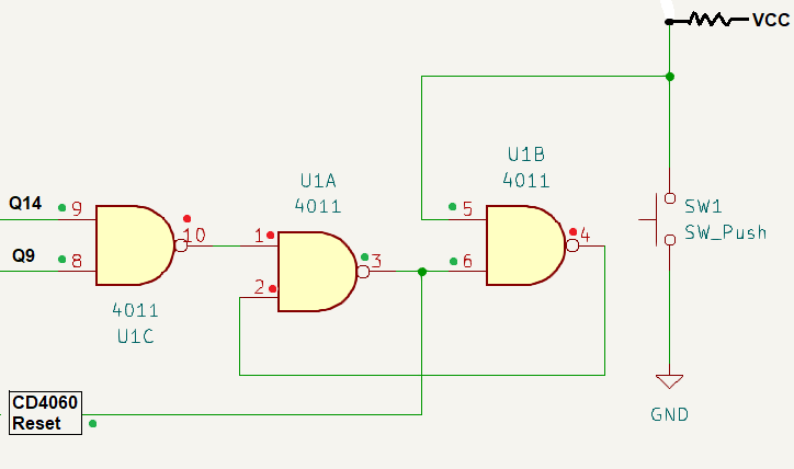
Because of the CD4060 reset, Q14 and Q9 will immediately go back to output LOW, which will set Pin 10 HIGH once again.
But this time, no more cascading effect, the middle NAND gate will no longer have both its input LOW but only one. Its output (Pin 3) will remain HIGH.
At that point, the system is now “stuck” in this state. Kind of a “Pause” state.
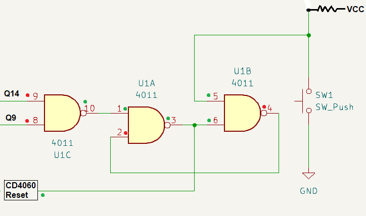
Look on the diagram below what happen as soon as the user press the push button SW1.
-
Pin 5 of the NAND gate at the right, will be immediately to LOW (because forced to GND through the push button), which cause its output to change from LOW to HIGH
-
As now both Pin 1 and Pin 2 of the middle NAND gate are HIGH, its output will be LOW, which will cause two follow up actions:
-
the reset pin of the CD4060 will be set back to LOW, causing the CD4060 to resume its normal operation.
-
Because now Pin 6 of the right NAND gate is set to LOW, it does not matter if the user is still pressing the button or not, Output (Pin 4) will be set to HIGH.
-
We are back on the initial state described at the beginning of this part.

At that point I think I have detailed all the steps describing how this little device work.
However something was bothering me, when I am testing it nowadays, the device is not marking the pause/sleep and goes back to counting even if I do not push the switch. It would appear that it is resetting on its own and that it is bound to endlessly loop between all the stages forever.
We will see that in the troubleshooting part (coming soon).